最近学了下stm32下的spi接口,感觉还是很强大的。为了测试,选了W25Qx系列的W25Q64BV这款spi flash芯片,64Mbit即8MB。使用STM32读写spi flash还是比较简单的,主要是发送一些指令等。spi芯片的应用还是很多,在一些低端路由上就把固件放在spi flash上,运行时把里面的数据读出放到ram里面运行。看来也可以用这个flash,在 stm32构建个嵌入式系统。
个人原创,转载请注明原文出处,并保留原文链接:
https://www.embbnux.com/2014/05/30/stm32_use_spi_write_w25q64_flash/
参考: stm32官方库 W25Q64数据手册
开发环境: UBUTNU LINUX ST官方库
一 W25Q64的一些命令表
这些在数据手册上可以查看到,进行什么操作就发送什么命令。
//W25Q64BV
#define W25Q64_DeviceID 0xEF16

#define W25X_CMD_WriteEnable 0x06 /*Write enable instruction */
#define W25X_CMD_WriteDisable 0x04 /*! Write to Memory Disable */
#define W25X_CMD_WriteStatusReg 0x01 /* Write Status Register instruction */

#define W25X_CMD_PageProgram 0x02 /* Write enable instruction */
#define W25X_CMD_QuadPageProgram 0x32 /* Write enable instruction */

#define W25X_CMD_BlockErase64 0xD8 /* Block 64k Erase instruction */
#define W25X_CMD_BlockErase32 0x52 /* Block 32k Erase instruction */
#define W25X_CMD_ChipErase 0xC7 /* Bulk Erase instruction */
#define W25X_CMD_SectorErase 0x20 /* Sector 4k Erase instruction */
#define W25X_CMD_EraseSuspend 0x75 /* Sector 4k Erase instruction */
#define W25X_CMD_EraseResume 0x7a /* Sector 4k Erase instruction */

#define W25X_CMD_ReadStatusReg1 0x05 /* Read Status Register instruction */
#define W25X_CMD_ReadStatusReg2 0x35 /* Read Status Register instruction */

#define W25X_CMD_High_Perform_Mode 0xa3
#define W25X_CMD_Conti_Read_Mode_Ret 0xff

#define W25X_WakeUp 0xAB
#define W25X_JedecDeviveID 0x9F /*Read identification */
#define W25X_ManufactDeviveID 0x90 /* Read identification */
#define W25X_ReadUniqueID 0x4B

#define W25X_Power_Down 0xB9 /*Sector 4k Erase instruction */

#define W25X_CMD_ReadData 0x03 /* Read from Memory instruction */
#define W25X_CMD_FastRead 0x0b /* Read from Memory instruction */
#define W25X_CMD_FastReadDualOut 0x3b /*Read from Memory instruction */
#define W25X_CMD_FastReadDualIO 0xBB /* Read from Memory instruction */
#define W25X_CMD_FastReadQuadOut 0x6b /* Read from Memory instruction */
#define W25X_CMD_FastReadQuadIO 0xeb /* Read from Memory instruction */
#define W25X_CMD_OctalWordRead 0xe3 /* Read from Memory instruction */

#define W25X_DUMMY_BYTE 0xff //0xA5
#define W25X_SPI_PAGESIZE 0x100
二 SPI底层初始化和操作程序
关于SPI接口我使用的是SPI2,具体和SPI1差不多
一些接口定义:
#define W25X_FLASH_SPI SPI2
#define W25X_FLASH_SPI_CLK RCC_APB1Periph_SPI2
#define W25X_FLASH_SPI_SCK_PIN GPIO_Pin_13 /* PB.13 */
#define W25X_FLASH_SPI_SCK_GPIO_PORT GPIOB /* GPIOB */
#define W25X_FLASH_SPI_SCK_GPIO_CLK RCC_APB2Periph_GPIOB
#define W25X_FLASH_SPI_MISO_PIN GPIO_Pin_14 /* PB.14 */
#define W25X_FLASH_SPI_MISO_GPIO_PORT GPIOB /* GPIOB */
#define W25X_FLASH_SPI_MISO_GPIO_CLK RCC_APB2Periph_GPIOB
#define W25X_FLASH_SPI_MOSI_PIN GPIO_Pin_15 /* PB.15 */
#define W25X_FLASH_SPI_MOSI_GPIO_PORT GPIOB /* GPIOB */
#define W25X_FLASH_SPI_MOSI_GPIO_CLK RCC_APB2Periph_GPIOB
#define W25X_FLASH_CS_PIN GPIO_Pin_12 /* PB.12 */
#define W25X_FLASH_CS_GPIO_PORT GPIOB /* GPIOB */
#define W25X_FLASH_CS_GPIO_CLK RCC_APB2Periph_GPIOB
SPI初始化:
//GPIO初始化
void SPI2_GPIO_Init(void){
 GPIO_InitTypeDef GPIO_InitStructure;

/*!< W25X_FLASH_SPI_CS_GPIO, W25X_FLASH_SPI_MOSI_GPIO, W25X_FLASH_SPI_MISO_GPIO
 and W25X_FLASH_SPI_SCK_GPIO Periph clock enable */
 RCC_APB2PeriphClockCmd(W25X_FLASH_CS_GPIO_CLK | W25X_FLASH_SPI_MOSI_GPIO_CLK | W25X_FLASH_SPI_MISO_GPIO_CLK |
 W25X_FLASH_SPI_SCK_GPIO_CLK, ENABLE);

 /*!< W25X_FLASH_SPI Periph clock enable */
 RCC_APB2PeriphClockCmd(W25X_FLASH_SPI_CLK, ENABLE); //

 /*!< Configure W25X_FLASH_SPI pins: SCK */
 GPIO_InitStructure.GPIO_Pin = W25X_FLASH_SPI_SCK_PIN;
 GPIO_InitStructure.GPIO_Speed = GPIO_Speed_50MHz;
 GPIO_InitStructure.GPIO_Mode = GPIO_Mode_AF_PP;
 GPIO_Init(W25X_FLASH_SPI_SCK_GPIO_PORT, &GPIO_InitStructure);

/*!< Configure W25X_FLASH_SPI pins: MOSI */
 GPIO_InitStructure.GPIO_Pin = W25X_FLASH_SPI_MOSI_PIN;
 GPIO_Init(W25X_FLASH_SPI_MOSI_GPIO_PORT, &GPIO_InitStructure);

/*!< Configure W25X_FLASH_SPI pins: MISO */
 GPIO_InitStructure.GPIO_Pin = W25X_FLASH_SPI_MISO_PIN;
 GPIO_InitStructure.GPIO_Mode = GPIO_Mode_IN_FLOATING;
 GPIO_Init(W25X_FLASH_SPI_MISO_GPIO_PORT, &GPIO_InitStructure);

 /*!< Configure W25X_FLASH_CS_PIN pin: W25X_FLASH Card CS pin */
 GPIO_InitStructure.GPIO_Pin = W25X_FLASH_CS_PIN;
 GPIO_InitStructure.GPIO_Mode = GPIO_Mode_Out_PP;
 GPIO_Init(W25X_FLASH_CS_GPIO_PORT, &GPIO_InitStructure);

}

//SPI2初始化
void SPI_Flash_Init(void){
 SPI_InitTypeDef SPI_InitStructure;

 SPI2_GPIO_Init();

 /*!< Deselect the FLASH: Chip Select high */
 W25X_FLASH_CS_HIGH();

 /*!< SPI configuration */
 SPI_InitStructure.SPI_Direction = SPI_Direction_2Lines_FullDuplex;
 SPI_InitStructure.SPI_Mode = SPI_Mode_Master;
 SPI_InitStructure.SPI_DataSize = SPI_DataSize_8b;
 SPI_InitStructure.SPI_CPOL = SPI_CPOL_High;
 SPI_InitStructure.SPI_CPHA = SPI_CPHA_2Edge;
 SPI_InitStructure.SPI_NSS = SPI_NSS_Soft;

 SPI_InitStructure.SPI_BaudRatePrescaler = SPI_BaudRatePrescaler_128;

 SPI_InitStructure.SPI_FirstBit = SPI_FirstBit_MSB;
 SPI_InitStructure.SPI_CRCPolynomial = 7;
 SPI_Init(W25X_FLASH_SPI, &SPI_InitStructure);

 /*!< Enable the W25X_FLASH_SPI */
 SPI_Cmd(W25X_FLASH_SPI, ENABLE);
 SPI_Flash_SendByte(0xff);
}
底层接口,发送字节,接受字节
//发送字节
uint8_t SPI_Flash_SendByte(uint8_t byte)
{
/*! Loop while DR register in not emplty */
while (SPI_I2S_GetFlagStatus(W25X_FLASH_SPI, SPI_I2S_FLAG_TXE) == RESET);

/*!Send byte through the SPI1 peripheral */
SPI_I2S_SendData(W25X_FLASH_SPI, byte);

/*! Wait to receive a byte */
while (SPI_I2S_GetFlagStatus(W25X_FLASH_SPI, SPI_I2S_FLAG_RXNE) == RESET);

/*! Return the byte read from the SPI bus */
return SPI_I2S_ReceiveData(W25X_FLASH_SPI);
}

//读取字节
uint8_t SPI_Flash_ReadByte(void)
{
return (SPI_Flash_SendByte(W25X_DUMMY_BYTE));
}
三 对SPI FLASH的上层读写操作程序
这部分对于flash来说大同小异,主要是对块和扇区的操作
//读取设备ID

uint16_t SPI_Flash_ReadID(void)
{
uint16_t Temp = 0, Temp0 = 0,Temp1 = 0;

/*Select the FLASH: Chip Select low */
W25X_FLASH_CS_LOW();

/*! Send "RDID " instruction */
SPI_Flash_SendByte(W25X_ManufactDeviveID);
SPI_Flash_SendByte(0x00);
SPI_Flash_SendByte(0x00);
SPI_Flash_SendByte(0x00);
/*! Read a byte from the FLASH */
Temp0 = SPI_Flash_SendByte(W25X_DUMMY_BYTE);

/*!< Read a byte from the FLASH */
Temp1 = SPI_Flash_SendByte(W25X_DUMMY_BYTE);
/*!< Deselect the FLASH: Chip Select high */
W25X_FLASH_CS_HIGH();

Temp = (Temp0 << 8) | Temp1;

return Temp;
}

//写一页256字节内。
void SPI_Flash_WritePage(uint8_t* pBuffer, uint32_t WriteAddr, uint16_t NumByteToWrite)
{
/* Enable the write access to the FLASH */
SPI_Flash_Write_Enable();

/* Select the FLASH: Chip Select low */
W25X_FLASH_CS_LOW();
/* Send "Write to Memory " instruction */
SPI_Flash_SendByte(W25X_CMD_PageProgram);
/*Send WriteAddr high nibble address byte to write to */
SPI_Flash_SendByte((WriteAddr & 0xFF0000) ;
/* Send WriteAddr medium nibble address byte to write to */
SPI_Flash_SendByte((WriteAddr & 0xFF00);
/* Send WriteAddr low nibble address byte to write to */
SPI_Flash_SendByte(WriteAddr & 0xFF);

/* while there is data to be written on the FLASH */
while (NumByteToWrite--)
{
/* Send the current byte */
SPI_Flash_SendByte(*pBuffer);
/* Point on the next byte to be written */
pBuffer++;
}

/*Deselect the FLASH: Chip Select high */
W25X_FLASH_CS_HIGH();

/* Wait the end of Flash writing */
SPI_Flash_WaitForWriteEnd();
}

//读
void SPI_Flash_ReadBuffer(uint8_t* pBuffer, uint32_t ReadAddr, uint16_t NumByteToRead)
{
/*Select the FLASH: Chip Select low */
W25X_FLASH_CS_LOW();

/*Send "Read from Memory " instruction */
SPI_Flash_SendByte(W25X_CMD_ReadData);

/*!< Send ReadAddr high nibble address byte to read from */
SPI_Flash_SendByte((ReadAddr & 0xFF0000);
/*!< Send ReadAddr medium nibble address byte to read from */
SPI_Flash_SendByte((ReadAddr& 0xFF00);
/*!< Send ReadAddr low nibble address byte to read from */
SPI_Flash_SendByte(ReadAddr & 0xFF);

while (NumByteToRead--) /* while there is data to be read */
{
/*!< Read a byte from the FLASH */
*pBuffer = SPI_Flash_SendByte(W25X_DUMMY_BYTE);
/*!< Point to the next location where the byte read will be saved */
pBuffer++;
}

/*!< Deselect the FLASH: Chip Select high */
W25X_FLASH_CS_HIGH();
}

void SPI_Flash_EraseChip(void)
{
/*!< Send write enable instruction */
SPI_Flash_Write_Enable();
SPI_Flash_WaitForWriteEnd();
/*!< Bulk Erase */
/*!< Select the FLASH: Chip Select low */
W25X_FLASH_CS_LOW();
/*!< Send Bulk Erase instruction */
SPI_Flash_SendByte(W25X_CMD_ChipErase);
/*!< Deselect the FLASH: Chip Select high */
W25X_FLASH_CS_HIGH();

/*!< Wait the end of Flash writing */
SPI_Flash_WaitForWriteEnd();
}
四 测试程序
测试是否能够连通,以及写入读出操作:
/*******************************************************

*************SPI测试程序*********************************

*************Author: Embbnux JI***************************

*************http://www.embbnux.com*********************

*******************************************************/

#include "stm32f10x.h";
#include "led.h";
#include "spi_flash.h";
#include "delay.h";
#include "usart.h";

uint8_t mem_buffer[] = {"Welcome to www.embbnux.com !"};
#define mem_size sizeof(mem_buffer)

int main(int argc, char *argv[])
{

uint32_t runcount=0;
uint8_t led_state=1;
uint8_t databuffer[mem_size];
//uint8_t ledtime=0;
rcc_config();
usart_init();
usart_send_string("\nsystem init start!");
delay_init(72);
led_init(LD_PORT,LD1,1);

//led_ctrl(LD_PORT,LD1,0);
delay_ms(500);
SPI_Flash_Init();
delay_ms(500);
led_ctrl(LD_PORT,LD1,0);
delay_ms(500);
usart_send_string("\nsystem init finish!");

if(SPI_Flash_ReadID()==W25Q64_DeviceID){

usart_send_string("\nflash init ok!");
}
else
{

usart_send_string("\nflash init fail!");
}
//擦除芯片 40s
SPI_Flash_EraseChip();
usart_send_string("\nflash erase success!");

//往芯片内写入数据
SPI_Flash_WritePage((uint8_t*)mem_buffer,1024,mem_size);
usart_send_string("\nflash write data success!\n");

//从芯片读取数据
SPI_Flash_ReadBuffer(databuffer,1024,mem_size);
usart_send_string((char*)databuffer);

while(1)
{

runcount++;
//led闪烁
if(runcount>=2000000){

led_ctrl(LD_PORT,LD1,led_state);
led_state++;
runcount=0;
if(led_state>=2) led_state=0;

}

}
}
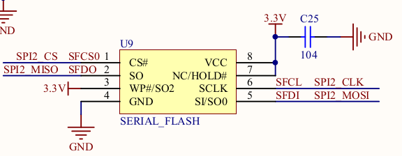
五 W25Q64BV电路图
再接下来就是在它上面构建fat文件系统了。
状态寄存器1和2有什么区别?
就是两个寄存器,各有各的功能,具体每个位你看下数据手册